Silicon-Germanium Research Program
J.D. Cressler
The emerging wireless communications market is projected to grow rapidly world
wide from a value of $25B by 1992 to roughly $200B by 2005. Wireless communications
will be incorporated into the Global Grid (commercial) and Tactical Theater
(military) networks over the next decade, and thus is clearly emerging as
a "dual-use" technology of strategic importance. At present, the
costs associated with radio-frequency (RF) circuitry in the mobile terminal
is a major barrier to the widespread dissemination of wireless communications
systems and personal communications devices. With the recent introduction
of silicon-germaniunm (SiGe) alloys, however, it will soon become practical to
replace more expensive Gallium-Arsenide (GaAs) RF circuits with SiGe circuits
having comparable performance at the significantly lower cost normally associated
with silicon manufacturing. Thus, SiGe technology is expected to accelerate the
merger of battery-powered communications equipment and computers and will help the
U.S. maintain its preeminence in the Information Age.
Having the
ability to practice bandgap engineering within the silicon (Si) material system
has long been a dream of semiconductor device designers. If realized, such techniques
would bring together the superior device properties of III-V heterojunction
bipolar transistors (HBT's) and the processing maturity of Si technology. Designers
would have the best of both worlds. This dream became reality with the introduction
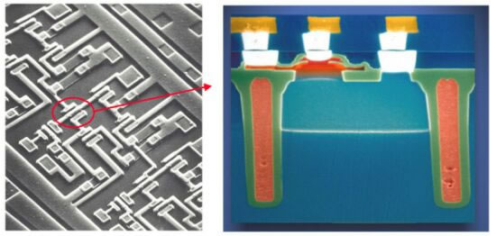
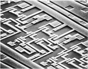
of SiGe growth techniques in the late 1980's. In the SiGe HBT, Ge is selectively
introduced into the base region of the transistor. The smaller base bandgap
of SiGe compared to Si enhances electron injection, producing a higher current
gain for the same base doping level compared to a Si device. Thus, the base
can be doped more heavily in the SiGe HBT in order to lower the total base resistance.
At the same time, using the ultrahigh vacuum / chemical vapor deposition (UHV/CVD)
growth technique allows the Ge content to be controllably graded across the
base to introduce a carrier drift-field and thereby improve the transistor frequency
response. In short, in terms of both frequency response and circuit delay, a
much faster device is obtained using SiGe.
The progress in this field has been both exciting and exceptionally rapid, beginning
with the first reported SiGe HBT in 1987, the clear demonstration of the performance
leverage over Si with the report in 1990 of a SiGe HBT having a 75 GHz cutoff
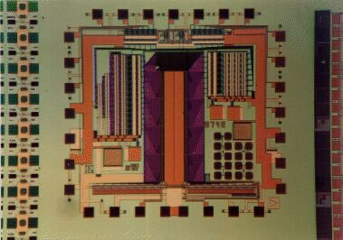
frequency, and continuing in 1992 with a full BiCMOS technology which integrated
SiGe HBT's with record performance (18 psec ECL gate delay) together with 0.25
micro-meters CMOS devices. Record peak cutoff frequency above 300 Ghz
have been achieved in 2004. Research in both devices and material growth techniques
continues at a very rapid pace in a number of industrial and university labs
around the world.
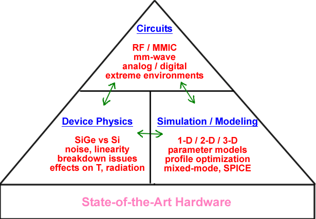
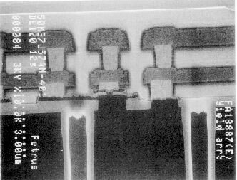
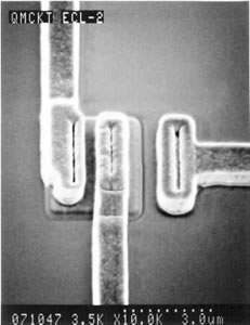
Dr. Cressler's SiGe research program addresses the fundamental physics, design, and modeling of SiGe bipolar transistors for these emerging wireless communications applications, and has strong financial support from both government and industrial sponsors. A university-industry-government partnership ensures that the results of research will have a timely impact on the developments in the wireless communications market.