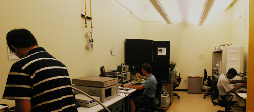
Exhaustive Device and Circuit Characterization Capabilities
- All Device Simulation Tools and Circuit Design Suites
- Integrated S-parameter + Noise Figure + Load-Pull System to 40 GHz
- SP + NF + 2-tone Linearity + Phase Noise + High Power to 67 GHz
- 75-110 GHz Circuit Measurement Capability (50ohm gain + noise + linearity)
- Close-in Phase Noise + AM-PM Test System (to 18 GHz)
- 4K - 400K dc to 40 GHz RF Cryogenic Test System
- Two 10K - 400K dc to 100 MHz Cyrogenic Test Systems
- 300°C High-Power Test System + Pulsed I-V Test System
- 1/f Noise Test System + Reliability/Stress Test System
- Five Semiconductor Parameter Analyzers + 12 GHz realtime scope
- Radiation Experiments + PCBs + High Speed Packaging + Wirebonding

Key Measurement Systems
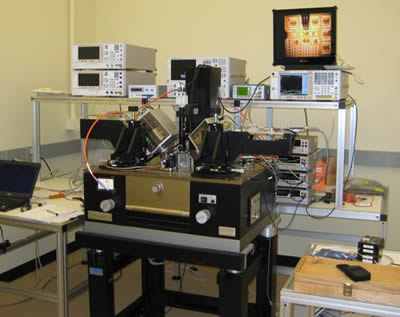
Integrated on-wafer S-parameter, Load-pull, and Noise Figure Station

- 45 MHz - 40 GHz S-parameter measurments
- 8 - 40 GHz Load-pull measurement, reaching < 4 ohms at 10 GHz
- 2 - 40 GHz Noise Figure measurement in EMI shield
- Custom Tuners, integration, and software provided by Focus Microwaves
- Modified Suss Microtech PM-8 probe station, with probe shield with capabilities for 8 inch wafer
- Agilent technologies RF measurement equipment including PNA, PSG, and PSA
Other Test Systems
- on-wafer dc systems for analysis down to 1 fA (15 K – 500 ºC)
- low-frequency noise (0.1 Hz – 100 kHz)
- phase noise systems (18 GHz)
- S-parameters (26 GHz and 110 GHz)
- load-pull (18 GHz)
- pulsed load-pull (18 GHz)
- ATN noise system (26 GHz)
- cryogenic dc + ac measurements on-wafer or packaged to 15 K
- automated C-V + I-V analysis system
- pulsed I-V (100 V / 2 A) system
- high-power / high-temperature test system (10 A, 1.1 kV, 500 ºC)
Other Resources
- all major simulation packages (Cadence, ADS, MEDICI, ISE, SUPREM ...)
- advanced semiconductor fabrication facilities (materials, devices, MEMS, etc.)
- advanced packaging facilities (MCM, flip-chip, etc.)
- extensive materials characterization (SIMS, SEM, TEM, DLTS, XRD, etc.


